Vous êtes ici
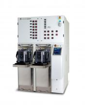
VertaCure Series
The YES-VertaCure automated, high temperature cure series of ovens is designed for today’s most demanding MEMS and semiconductor process applications. Whether it’s for proper curing of multiple layers of polyimide in an RDL (Bond Pad Re-routing) application or annealing copper in an advanced semiconductor device, the YES-VertaCure helps achieve total environmental control to increase yields and extend device performance.
The system incorporates the laminar flow technology of the YES-450PB series. It accommodates 200 and 300mm wafers with one or two load ports and a wafer handling robot inside an integrated Class 1 minienvironment. Up to 50 wafers are loaded into a stainless steel cassette-type rack on the oven chamber door and, when loading is complete, lifted up into the vacuum chamber.
Applications
(YES-VertaCure)
- Polyimide cure
- Copper anneal
- BCB cure
- Low-k dielectric cure
High Vacuum Option
(YES-VertaVac)
- Wafer dehydration
- Getter activation
- Gas desorption
- Metal annealing
- Thin film resistors thermal treatments
Silane Vapor Deposition Option
(YES-VertaCoat)
- Porous dielectric repair
- Copper to low-k adhesion repair
- Copper anti-oxidation barrier
- Copper oxide removal
- Copper diffusion barrier
- Moisture removal/film sealing
- Imprint lithography surface adhesion control
- Hydrophobic sealing
Ideal Process Environment
VertaCure Series is designed to achieve tight control over your process atmosphere:
- Maximum process temperature up to 450ºC
- Controlled ramp up and cool down
- Extremely low oxygen process concentrations
- Low--or no--particle addition
- Fully automated
- Touch screen interface
- Horizontal laminar flow for increased particle isolation and removal (for most cure processes, average particle addition is negative)
MEMS Applications
The VertaCure Series is available with:
- High vacuum
- Vapor deposition
Which supports the following MEMS applications:
- Metal Annealing
- Annealing is a heat treatment where the microstructure of a material is altered, causing changes in its properties such as strength and hardness. In the semiconductor industry, silicon wafers are annealed so that dopant atoms (such as boron, phosphorus or arsenic), can be incorporated into substitutional positions into the crystal lattice, which drastically changes the electrical properties of the semiconducting material. In the case of copper, adding an anneal step:
- Improves properties of the copper layer
- Increases grain size for faster polishing
- Provides better conductivity
- Reduces surface tension
- Minimizes electromigration
- Allows a consistent CMP rate across the wafer
- Wafer dehydration
- The moisture on the surface of wafers will cause unintended reactions with various deposition steps. These reactions result in unstable surface which degrade over time. Vacuum dehydration provides a clean stable starting surface resulting in superior films.
- Getter Activation
- Getters are used to scavenge unwanted gases in many applications. In MEMS devices, getters may be used to tie up excess moisture or hydrogen which may interfere with the long term operation of the device. Activating the getter material involves high temperature and high vacuum processing to ensure the material starts as moisture / hydrogen-free as possible.
- Thermal treatment of Thin Film Resistors
- Thin film resistors can change properties rapidly as they age unless they are properly thermally treated. The process stabilizes the crystal grain and ensures long term predictable behavior.
- Surface Tension Modification
- As devices are made smaller and smaller, static friction (stiction) becomes more and more significant. By modifying the surface tension with a class of fluorinated silanes, the operating life of moving parts in MEMS devices can be significantly lengthened. Conversely, if surfaces need to be bonded together, other silanes can be coated which enhance bonding strengths between unlike materials.
Process Cycle
YES-VertaCure Process
The process begins with vacuum cycle purges to remove oxygen and water vapor followed by a continuous horizontal laminar flow of up to four process gases. The laminar flow of gas can be maintained during a recipe-driven temperature profile. Operating temperatures are 150°C to 450°C; pressure range is 50-500 Torr.
YES-VertaVac (High Vacuum Process)
The process begins with vacuum cycle purges to remove oxygen and water vapor followed by a continuous horizontal laminar flow of up to four process gasses. The laminar flow of gas can be maintained during a recipe-driven temperature profile. Operating temperatures are 150°C to 450°C; laminar flow pressure range is 0.50-500 Torr. The tool is also capable of evacuation down to 5E-5 Torr using a vacuum turbo pump.
The YES-VertaVac gives engineers moisture resistant surface modification and increased time available between process steps.
YES-VertaCoat (Silane Vapor Deposition Process)
Silane vapor deposition is a process that assists in the de position of a thin film of various chemistries in order to achieve precise surface modification. Vapor deposition is the preferred method for coating surfaces with silanes.
As technology shrinks, there is a growing need for precise control over nanoscale surface areas. The YES-VertaCoat gives you total control over your process environment. The tool also is designed as a flexible system to accom modate a variety of silanes and processes.
Specifically, the silane vapor deposition process assists with MEMS coating to reduce damaging stiction and photoresist adhesion for semiconductor wafers. The entire YES-VertaCure series is designed to give you uniform, repeatable results with an added bonus of cost savings!